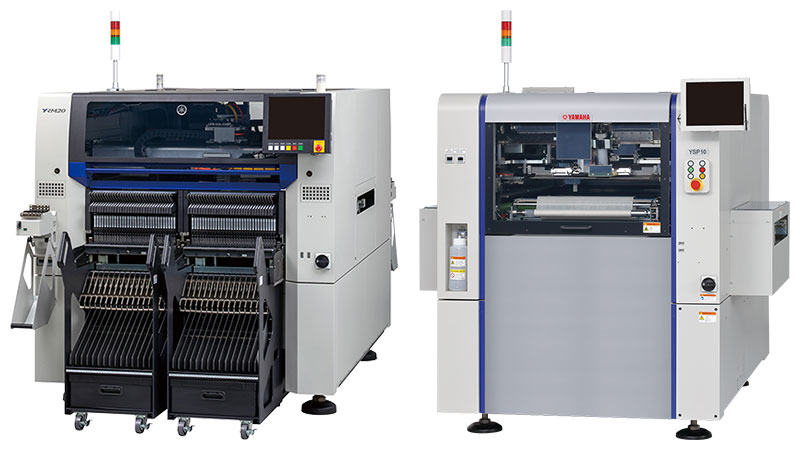
【Discontinued Product】High-Speed & High-Accuracy Flip Chip Bonder YSB55w Specifications, External dimension
High bonding accuracy and x3 productivity of conventional machines! This brings a New Era in Semiconductor packaging for the expanding flip chip market.
Specifications
| YSB55w | |||
|---|---|---|---|
| Applicable substrate | L240 x W200 to L50 x W50mm | ||
| Substrate thickness | 0.2 to 3.0mm | ||
| Transport direction | Left to Right (option : Right to Left) | ||
| Bonding accuracy | ±5µm (3σ) (When using Yamaha's standard components) | ||
| Throughput | 13,000UPH (Including processing time) | ||
| Applicable wafer size | 12 inch wafer | ||
| Applicable die size | □2 to 30mm | ||
| Power supply | 3-Phase AC 200/208/220/240/380/400/416V ±10% 50/60Hz | ||
| Air supply | 0.45MPa or more | ||
| External dimension | L2,090 x D1,866 x H1,550mm (YSB55w main unit & wafer feed unit) | ||
| Weight | Approx. 3,600kg (YSB55w main unit & wafer feed unit) | ||
- Specifications and appearance are subject to change without prior notice.
External dimension


